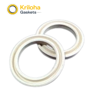
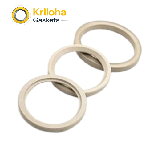
At Kriloha Ltd., we understand that in the semiconductor industry, “clean” is a relative term—perfection is the only standard. Our PEEK Rings for Semiconductors represent our engineered answer for “Contamination-Zero-Security” and “Vacuum-Integrity-Stability.” As a premier manufacturer of high-performance polymer solutions, Kriloha has established a “Clean-Room-Focused” fabrication protocol to ensure that every ring meets the stringent requirements of modern fab environments.
The engineering of our semiconductor ring program is founded on Material-Purity and Surface-Roughness ($R_a$) Optimization. By utilizing state-of-the-art 5-axis CNC machining, we eliminate the risk of “parting-line” debris and internal stresses associated with molding. At Kriloha, we verify the outgassing profiles and ionic purity of every batch, resulting in “Failure-Resistant” components that enable higher yields and longer maintenance intervals for your critical process tools.
Manufacturing these advanced polymer components involves strict Dimensional Verification, Plasma-Exposure Testing, and ESD-Calibration. We collaborate directly with your process engineers to develop bespoke configurations—including specialized “vent-grooves” for vacuum applications and proprietary geometries for wafer retention. By choosing Kriloha Ltd., you are investing in a “Future-Proof” manufacturing partnership that prioritizes your yield through superior material science.